
Advantage and Core Benefit
•Failsafe Design for Over-Input Protection
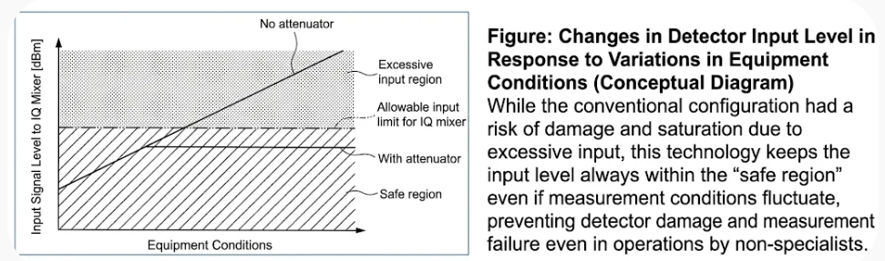
A unique structural design blocks excessive input, safeguarding detectors and preventing equipment downtime even when operated by non-experts.
•Unwavering Measurement Reproducibility
By eliminating the need for delicate manual input adjustments, this system removes operator skill dependencies, consistently delivering stable measurement data.
•Accelerated On-Site Optimization via Non-Contact Measurement
Capable of directly measuring absolute density without the plasma disturbance typical of probe methods. This accelerates the optimization of manufacturing conditions, freeing you from a reliance on empirical rules of thumb.
Background and Technology
In semiconductor manufacturing and similar fields, plasma density has often been managed through empirical rules of thumb, making quantitative process evaluation a significant challenge. While conventional non-contact microwave interferometers offer high precision, their signal input adjustments are notoriously delicate. The constant risk of detector damage and data inconsistency due to operational errors has hindered their widespread adoption on the factory floor.
This new technology overcomes these hurdles by structurally blocking excessive input through a proprietary failsafe design. Even operators without specialized high-frequency expertise can safely run measurements with the flip of a switch, achieving highly reproducible and flawless electron density measurements.
Partnaring Model
【Invitation for Technology Introduction & Joint Development】
Commissioned by the University of Tsukuba, Tech Manage Corp. is seeking corporate partners interested in adopting and commercializing this non-contact plasma diagnostic technology. We are highly interested in collaborating with companies seeking to use this system as an in-house evaluation tool in their R&D and manufacturing sites, or to integrate it as a standard feature or optional module in their own equipment line.
Ideal Partners:
Companies looking to introduce a safe, robust measurement environment where non-experts can operate the system without exceeding detector limits or causing equipment damage. (This includes equipment manufacturers looking to embed in-line diagnostic functions).
We offer direct technical consultations and discussions (online available) with the inventors. Upon signing a Non-Disclosure Agreement (NDA) with the University of Tsukuba, we are ready to disclose the full patent application, unpublished measurement data, and specific design parameters for the over-input protection circuit. We welcome your inquiries.
Principal Investigator
Associate Professor Masashi Yoshikawa (Faculty of Pure and Applied Sciences, University of Tsukuba)
Patents and Publications
Patent Pending